Search
 中文
中文


- Epitixial Wafer Growth
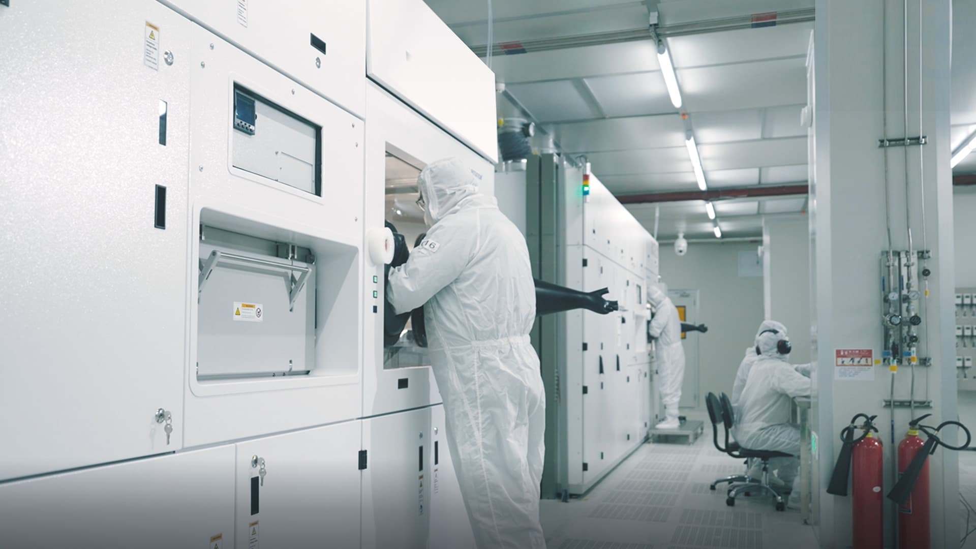
- Wafer Fabrication
- Chip Packaging
- Chip Testing

Utilizes advanced MOCVD systems to produce epitaxial wafers for laser light source chips, offering foundry and customized growth services for 2- 6 inch wafers.
Capable of independently growing GaAs- and InP-based materials and epitaxial structures for edge-emitting and VCSEL devices.
Capable of characterizing epitaxial structures, including wavelength, composition, and doping profiles.
-
Photolithography/Etching
Photolithography: UV lithography, nano-imprint lithography
Etching: Dry etching, wet etching
-
Thin-Film Deposition
Insulating Films: SiO₂, Si₃N₄, Al₂O₃, HfO₂
Metal Films: Ti, Pt, Au, AuGe, Ni, Ge, Cr, etc.
Deposition Techniques: Evaporation, sputtering, electroplating
-
Ion Implantation
Wafer Sizes: 4-inch, 6-inch, and small pieces
Energy Range: 30–380 keV (single charge)
Implant Species: H⁺, He⁺
-
Wafer Dicing & Facet Coating
Coating Materials: SiO₂, Al₂O₃, Ta₂O₅, Nb₂O₅, Ti₃O₅, Si
Reflectance Range: 0.1%–99%
-
Thinning & Polishing
GaAs and InP substrates
-
Wet Thermal Oxidation
Process: Al(Ga)As wet N₂ oxidation
Wafer Sizes: 4-inch, 6-inch, and small pieces
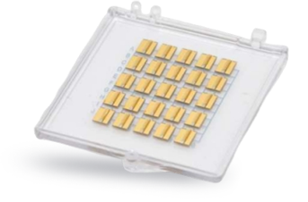
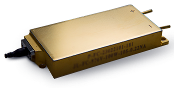
We offers a wide spectrum of customizable packaging solutions—including TO, COC, COS, C-Mount, CS, and F-Mount packages, as well as fiber-coupled modules—precisely tailored to the specific requirements of diverse applications.
-
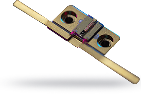
COS Module
-
F-MOUNT Module
-
Fiber Coupled Module
-
Fiber Coupled Diode Laser
System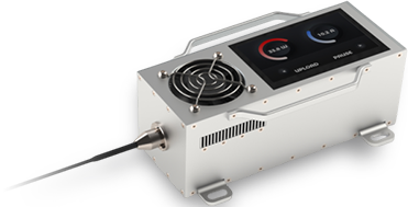
-
COC Module
-
1
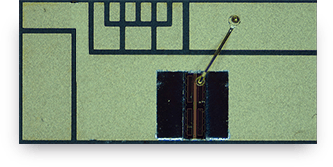
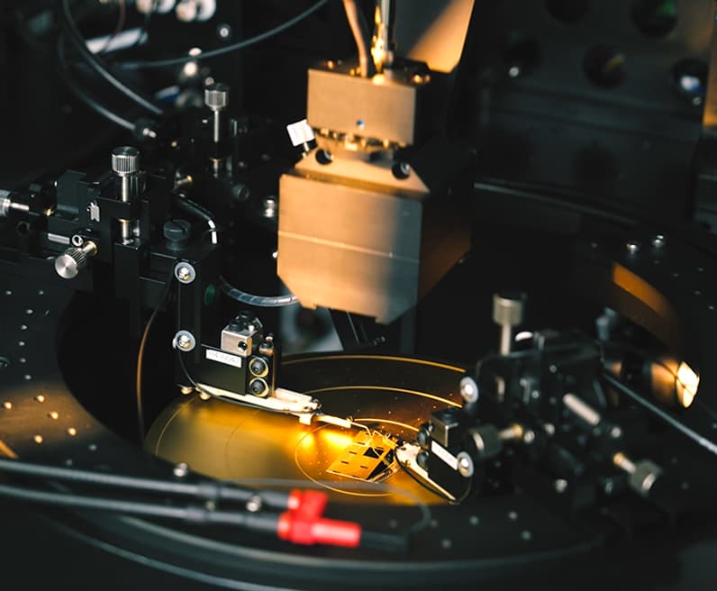
Automated Chip Testing
Automated Probing & Sorting for 4-6 inch VCSEL Wafers
-
2
High-Frequency Device Testing
Small-signal Characterization
Large-signal Characterization
RIN (Relative Intensity Noise) Measurement -
3
Reliability Testing
Real-time Aging Monitoring
Temperature Cycling From –40 °C to 85 °C
High-temperature, High-humidity Test (85°C/85 % RH)